Programmable Photonic Devices and Architectures for Machine Learning
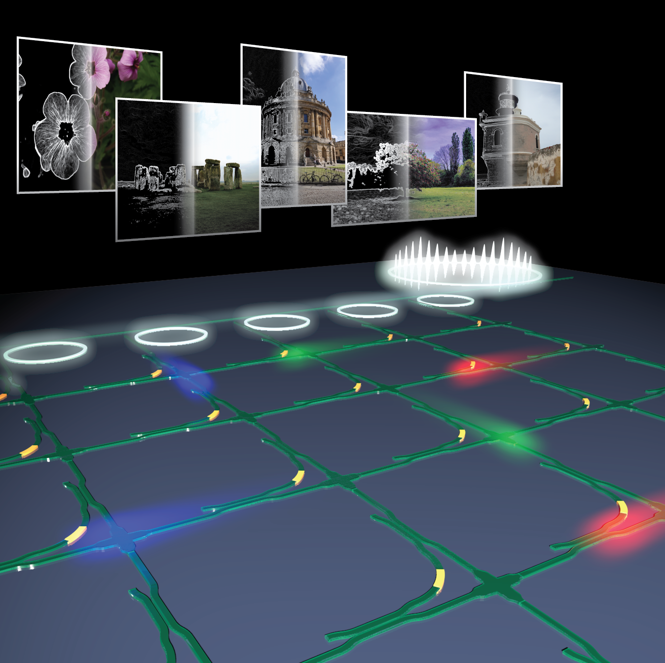
Optics has the unique ability to perform linear operations with (theoretically) no energy consumption. This allows for high-speed, low-energy matrix-vector multiplications in the optical domain. Since matrix multiplications form the basis for nearly all machine learning algorithms, hybrid hardware accelerators based on integrated photonics and electronics could significantly increase data throughput by leveraging the wavelength multiplexing and high modulation speeds of silicon photonics.
Waveguide-Integrated Circuits for Biosensing
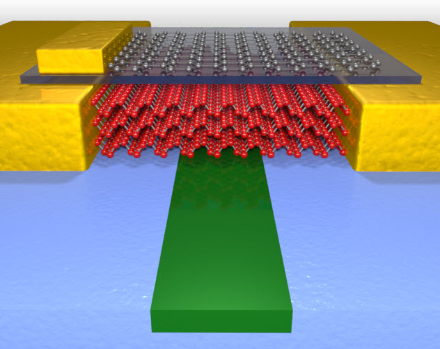
Combining plasmonics with integrated photonics allows for hybrid devices where we can overcome the high propagation loss of plasmonics and diffraction-limited dimensions of photonics. We have exploited this device geometry to enhance the performance of optoelectronic devices and are now interested in using what we have learned to achieve high-speed, low-concentration biosensing on-chip. (Image credit: Jacob Swett and Nick Farmakidis)
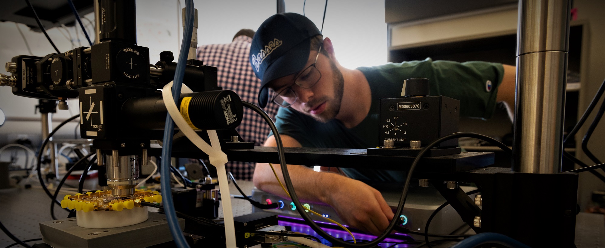
Waveguide-Integrated 2D Materials for High Performance Optoelectronics
The desirable optoelectronic properties of 2D materials such as graphene and black phosphorous, combined with their ability to be easily transferred to arbitrary substrates, make them a perfect canditate for integration with photonics. Placing 2D materials on top of a waveguide has the added benefit of overcoming the low out-of-plane absorption of these materials.